PCB Traces The Critical Role of Traces in PCB Design and Manufacturing Circuit Diagram The test works through the use of needles attached to a probe on an x-y grid obtained from basic CAD. Your ECM program coordinates to match the circuit board and then runs the program. In some cases, ICT makes it unnecessary to use flying probe testing, but the PCB has to be designed to fit with the test fixture -- which means a higher initial
Steps to Measure Voltage. Please turn on the device: First, ensure the PCB or the device it's part of is powered on.It would help if you had electricity flowing through the board to measure the voltage. Set your multimeter: Turn the multimeter dial to the voltage setting.Most digital circuits use DC voltage, so choose that setting.; Connect the probes: Touch the red probe to the positive point
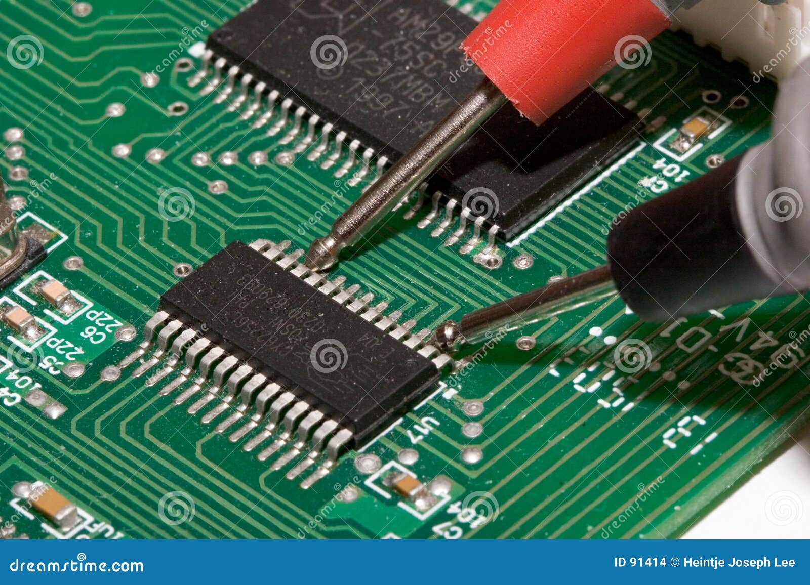
How to Use a Multimeter to Test Your PCB Board Circuit Diagram
Mastering PCB Testing: Techniques, Methods, and Best Practices Unveiled test, an X-ray technician can find flaws early in the production process by scrutinizing solder connections, internal traces, and barrels. Inspectingnspect components out of sight using X-ray inspection, like connectors and ball grid array packages with solder joints
Strong adhesion between the copper traces and the PCB substrate is crucial for the durability and reliability of the board. The Peel Test ensures that the copper traces will not separate from the substrate during manufacturing or operation, preventing electrical failures and extending the lifespan of the PCB. 21. Accelerated Life Testing (ALT)

Mastering PCB Testing: Techniques, Methods, and Best ... Circuit Diagram
The Litmus Test for PCB Reliability Predicting and ensuring the long-term performance of PCBs in the electronic manufacturing field is a challenge. Environmental Stress Screening (ESS) provides a powerful tool with its unique accelerated testing methods. By simulating harsh environmental conditions such as high temperatures, low temperatures